
Data Sheet

PCA9685 All information provided in this document is subject to legal disclaimers. © NXP B.V. 2010. All rights reserved.
Product data sheet Rev. 3 — 2 September 2010 25 of 51
NXP Semiconductors
PCA9685
16-channel, 12-bit PWM Fm+ I
2
C-bus LED controller
7.3.6 SUBADR1 to SUBADR3, I
2
C-bus subaddress 1 to 3
Subaddresses are programmable through the I
2
C-bus. Default power-up values are E2h,
E4h, E8h, and the device(s) will not acknowledge these addresses right after power-up
(the corresponding SUBx bit in MODE1 register is equal to 0).
Once subaddresses have been programmed to their right values, SUBx bits need to be
set to logic 1 in order to have the device acknowledging these addresses (MODE1
register).
Only the 7 MSBs representing the I
2
C-bus subaddress are valid. The LSB in SUBADRx
register is a read-only bit (0).
When SUBx is set to logic 1, the corresponding I
2
C-bus subaddress can be used during
either an I
2
C-bus read or write sequence.
7.3.7 ALLCALLADR, LED All Call I
2
C-bus address
The LED All Call I
2
C-bus address allows all the PCA9685s in the bus to be programmed
at the same time (ALLCALL bit in register MODE1 must be equal to 1 (power-up default
state)). This address is programmable through the I
2
C-bus and can be used during either
an I
2
C-bus read or write sequence. The register address can also be programmed as a
Sub Call.
Only the 7 MSBs representing the All Call I
2
C-bus address are valid. The LSB in
ALLCALLADR register is a read-only bit (0).
If ALLCALL bit = 0, the device does not acknowledge the address programmed in register
ALLCALLADR.
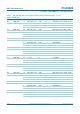
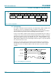
Table 8. SUBADR1 to SUBADR3 - I
2
C-bus subaddress registers 0 to 3 (address 02h to
04h) bit description
Legend: * default value.
Address Register Bit Symbol Access Value Description
02h SUBADR1 7:1 A1[7:1] R/W
1110 001*
I
2
C-bus subaddress 1
0 A1[0] R only
0*
reserved
03h SUBADR2 7:1 A2[7:1] R/W
1110 010*
I
2
C-bus subaddress 2
0 A2[0] R only
0*
reserved
04h SUBADR3 7:1 A3[7:1] R/W
1110 100*
I
2
C-bus subaddress 3
0 A3[0] R only
0*
reserved
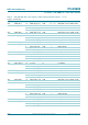
Table 9. ALLCALLADR - LED All Call I
2
C-bus address register (address 05h) bit
description
Legend: * default value.
Address Register Bit Symbol Access Value Description
05h ALLCALLADR 7:1 AC[7:1] R/W
1110 000*
ALLCALL I
2
C-bus
address register
0 AC[0] R only
0*
reserved