
User Manual


Embedded Controller TKS-G20-LN05 Rev.B
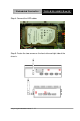
Chapter 2 Quick Installation Guide 2 - 9
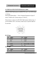
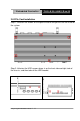
2.6 Digital I/O Connector (CN26)
This connector offers 4-pair of digital I/O function.
BIOS using the I2C Bus to read/write internal DIO registers and the Serial Bus
address is 0x6E.
The pin definitions are illustrated below:
Pin Signal Pin Signal
1 DIO_IN0 2 DIO_IN1
3 DIO_IN2 4 DIO_IN3
5 DIO_OUT0 6 DIO_OUT1
7 DIO_OUT2 8 DIO_OUT3
9 +3.3 Volt. 10 Ground
Note
: The max. rating of Pin 1 ~ Pin 8 is 3.3V@8mA
The max. rating of Pin 9 is 3.3V@0.5A
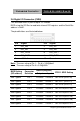
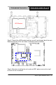
A
ddress(Register)
BIOS Setting
(I2C address)
Connector
Definition
Output Input
F75111 GPIO Setting
Port 1 @6Eh Pin 1 21h/Bit 0 22h/Bit 0 U67 Pin 6 (GPIO 20)
Port 2 @6Eh Pin 2 21h/Bit 1 22h/Bit 1 U67 Pin 7 (GPIO 21)
Port 3 @6Eh Pin 3 21h/Bit 2 22h/Bit 2 U67 Pin 8 (GPIO 22)
Port 4 @6Eh Pin 4 21h/Bit 3 22h/Bit 3 U67 Pin 24(GPIO 23)
Port 5 @6Eh Pin 5 21h/Bit 4 22h/Bit 4 U67 Pin 23(GPIO 24)
Port 6 @6Eh Pin 6 21h/Bit 5 22h/Bit 5 U67 Pin 22(GPIO 25)
Port 7 @6Eh Pin 7 21h/Bit 6 22h/Bit 6 U67 Pin 21(GPIO 26)
Port 8 @6Eh Pin 8 21h/Bit 7 22h/Bit 7 U67 Pin 20(GPIO 27)