
User Manual


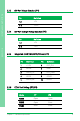
Table Of Contents
- Copyright Notice
- Acknowledgement
- Packing List
- About this Document
- Safety Precautions
- FCC Statement
- China RoHS Requirements (CN)
- China RoHS Requirement (EN)
- Table of Contents
- Chapter 1 - Product Specifications
- Chapter 2 – Hardware Information
- 2.1 Dimensions
- 2.2 Jumpers and Connectors
- 2.3 List of Jumpers
- 2.4 List of Connectors
- 2.4.1 RTC Battery Connector (CN1)
- 2.4.2 I-PEX Connector for Wi-Fi (CN2)
- 2.4.3 mPCIe Slot for WWAN Card (CN3H3)
- 2.4.4 Nano-SIM Slot (CN4)
- 2.4.5 RS-232/422/485 Port (D-Sub) (CN5)
- 2.4.6 USB 3.2 Gen 1 (Bottom)/ USB 2.0 (Top) Dual Port (CN6)
- 2.4.7 USB 3.2 Gen 1 Type C OTG (CN7)
- 2.4.8 Debug Port (CN8)
- 2.4.9 Gigabit Ethernet (GbE) Port (CN9)
- 2.4.11 eDP Connector (CN11)
- 2.4.13 HDMI 2.0 Port Type A (CN13)
- 2.4.14 Micro-SD Card Slot (CN14)
- 2.4.15 Speaker Connector (CN15)
- 2.4.16 DC Power Input (CN16)
- 2.4.19 Integrated USB, I2C x 2, 5V (CN19)
- 2.4.21 RS-232 Port (CN21)
- 2.4.22 GPIO Port (CN22)
- 2.5 Function Block
- Appendix A – Mating Connectors

Chapter 2 – Hardware Information 7
Rockchip RK3399 Platform
RICO-3399
2.3 List of Jumpers
Please refer to the table below for all of the board’s jumpers that you can configure for
your application
Label
Function
JP2
Power Button
JP3
RS-232/422/485 (D-Sub) Voltage Output Selection
JP4
eDP Port Voltage Selection
JP5
eDP Port Backlight Voltage Selection
JP6
Integrated (UART/I2C/GPIO/Others)
JP7/ JP8
COM port setting
SW1
Image Flash Switch
2.3.1 Power Button (JP2)
Pin
Definition
1
PWR_KEY#
2
GND
2.3.2 RS-232/422/485 (D-Sub) Voltage Output Selection (JP3)
Pin
Definition
1
12V
2
R1#/12V/5V
3
5V