
Instruction manual

61
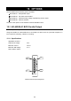
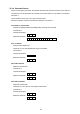
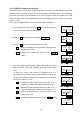
15-1-2 Equivalent circuit diagram
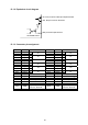
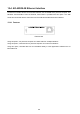
15-1-3 Connector pin assignment
Pin No. Direction BCD code Pin No. Direction BCD code
A1 Output 1 B1 Output 2
A2 Output 4
10
0
B2 Output 8
10
0
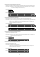
A3 Output 1 B3 Output 2
A4 Output 4
10
1
B4 Output 8
10
1
A5 Output 1 B5 Output 2
A6 Output 4
10
2
B6 Output 8
10
2
A7 Output 1 B7 Output 2
A8 Output 4
10
3
B8 Output 8
10
3
A9 Output 1 B9 Output 2
A10 Output 4
10
4
B10 Output 8
10
4
A11 Output 1 B11 Output 2
A12 Output 4
10
5
B12 Output 8
10
5
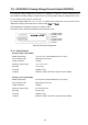
A13 Output OVER B13 Output Polarity
A14 Output STABLE B14 Output Zero band
A15 Output Decimal point 10
1
B15 Output Decimal point 10
2
A16 Output Decimal point 10
3
B16 Output Decimal point 10
4
A17 B17
A18 Output STROBE B18 Input HOLD
A19 COM
Input/output
common terminal
B19 COM
Input/output
common terminal
A20 FG Frame ground B20 FG Frame ground
+5V
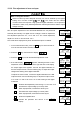
A
D-4532B interio
r
A
1 to A16, A18, B1 to B16 pin output terminals
A
19, B19 pin common terminals
B18 pin HOLD input terminal